This article is related to so-called “memory cards” (MC01) or SRAM cards. Mass storage cards (HD01) generally Just Work if your scope supports them.
I want to attempt to solidify information surrounding the use of memory cards (MC01 SRAM) in older LeCroy oscilloscopes such as the LC series, DDA series, 93xx series, and 94xx series. I hope to dispel some myths and confusion. I only own the LC574AL and would appreciate the results of using this information with other scopes if you try.
Note: “PCMCIA” and “PC Card” may be used interchangeably here to reference the same type of cards. PCMCIA was the original designation while PC Card is the newer naming convention.
MC01 PCMCIA specifications:
| Interface | Any directly addressable linear memory card1 |
| Data bus width | 8-bit only |
| Card attributes (aka CIS) | Not used2 |
| Voltage | 5V cards only |
| Access speed | 250ns3 |
| Filesystem | Firmware image or Raw DOS FAT (no partition) |
| Memory size | 64KB-64MB4 |
- The scope only supports simple access, direct reading and writing. If the memory card requires complex access such as required for writing to many flash devices then they will only work in read-only mode.
- Does not matter if the card has attributes or not, they will be ignored.
- Signalling speed is 3 MHz or 333ns. There is some overhead when measuring this so 250ns is the closest official PCMCIA speed.
- The scope will recognize cards formatted larger than 64MB however it is unclear if it is physically capable of accessing all the data since the PCMCIA specification only has 26 address lines.
Note these specifications are important even if using a genuine SRAM card. Not all of them will work. Especially important is whether or not it supports 8-bit mode (some can automatically switch). A 16-bit only SRAM card should be able to be hacked similar to a linear flash card (see below).
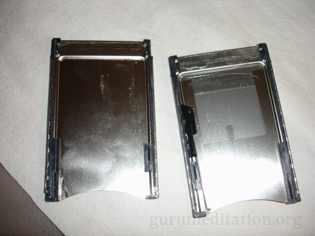
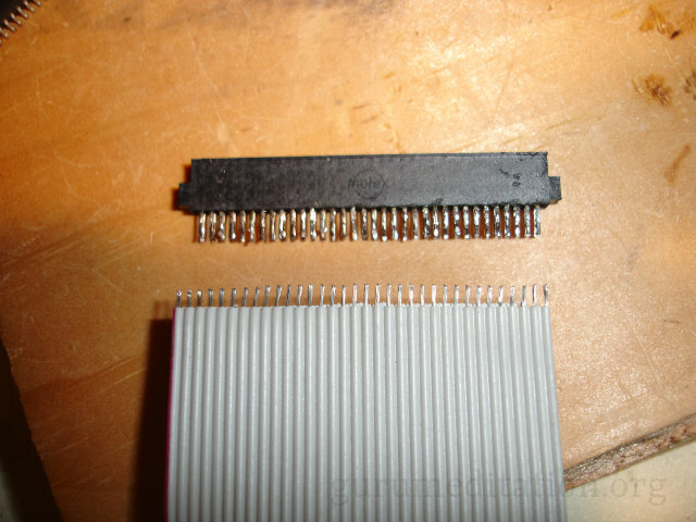
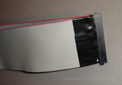
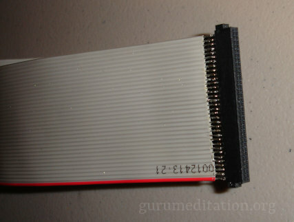
PCMCIA SRAM cards are absurdly priced (the motivation for this whole thing) and I could not find someone to help me test this so I had to build my own SRAM card to figure out how it works. I did this by breaking open an old PCMCIA card and removing its contents so I could use the PCMCIA socket connector and case for external connections. The pin count and spacing is the same as 34-pin floppy cables so I used those for my external interface. Note, if you want to use a 3V PCMCIA case then you will need to modify the “key” at the front of the card. 3V cards use a physically larger slot on the host and will not fit in to a 5V-only socket but with some grinding/cutting the key can be modified to fit.
This is my constructed PCMCIA card with external connections:
I used two 64KB SRAM chips pulled off of an old 586 PC motherboard, one for the common memory area and one for attributes. I only connected 8 address lines to the attribute memory for 128 bytes of storage (in attribute memory only even bytes are available). I did not need the attributes memory but it was useful for experimenting on PC based PCMCIA readers. I made a little Lua script to generate padded attributes data. It’s here if you want it. See the official specification for what goes in the tuple.
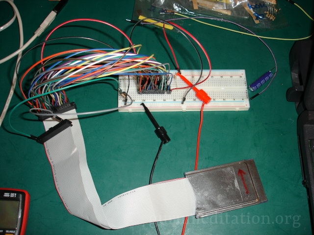
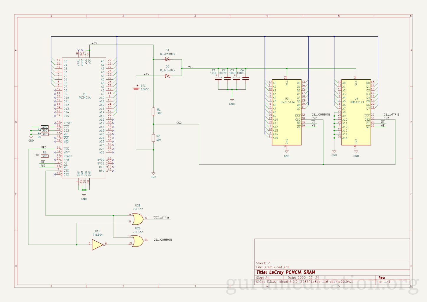
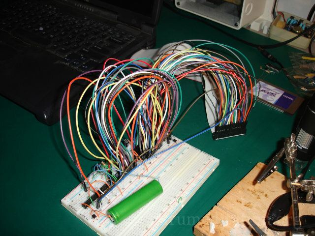
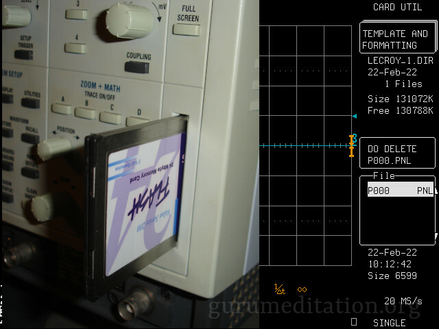
The scope will use an existing filesystem on the card to detect its size or when formatting a card it will try to write to various places on the card until it succeeds and therefore determines its size. This is the schematic and a picture of it built on a breadboard (lots of wires!):
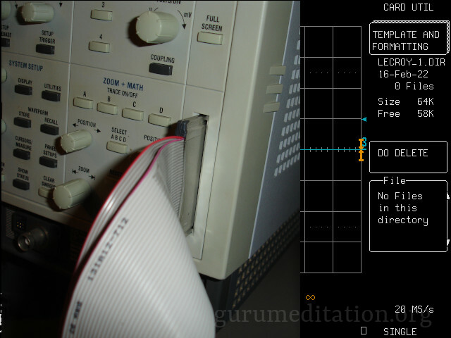
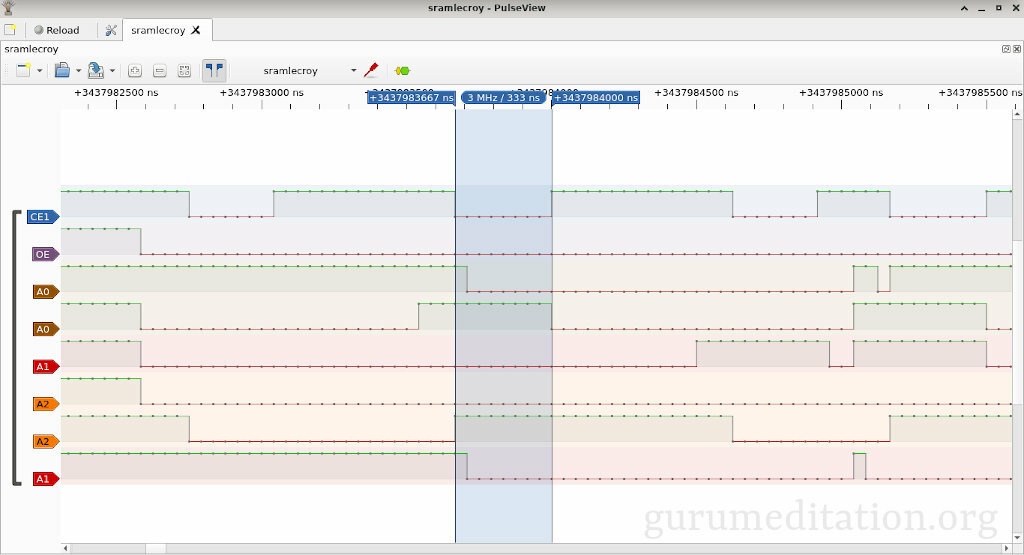
I used sigrok with a FX2 based logic analyzer and the scope itself to view the communication to the memory card: (sorry pulseview failed to load the labels properly but you get the idea)
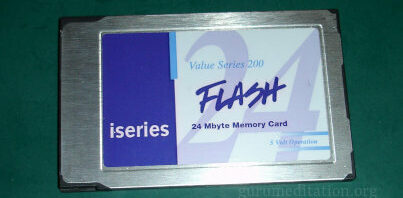
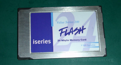
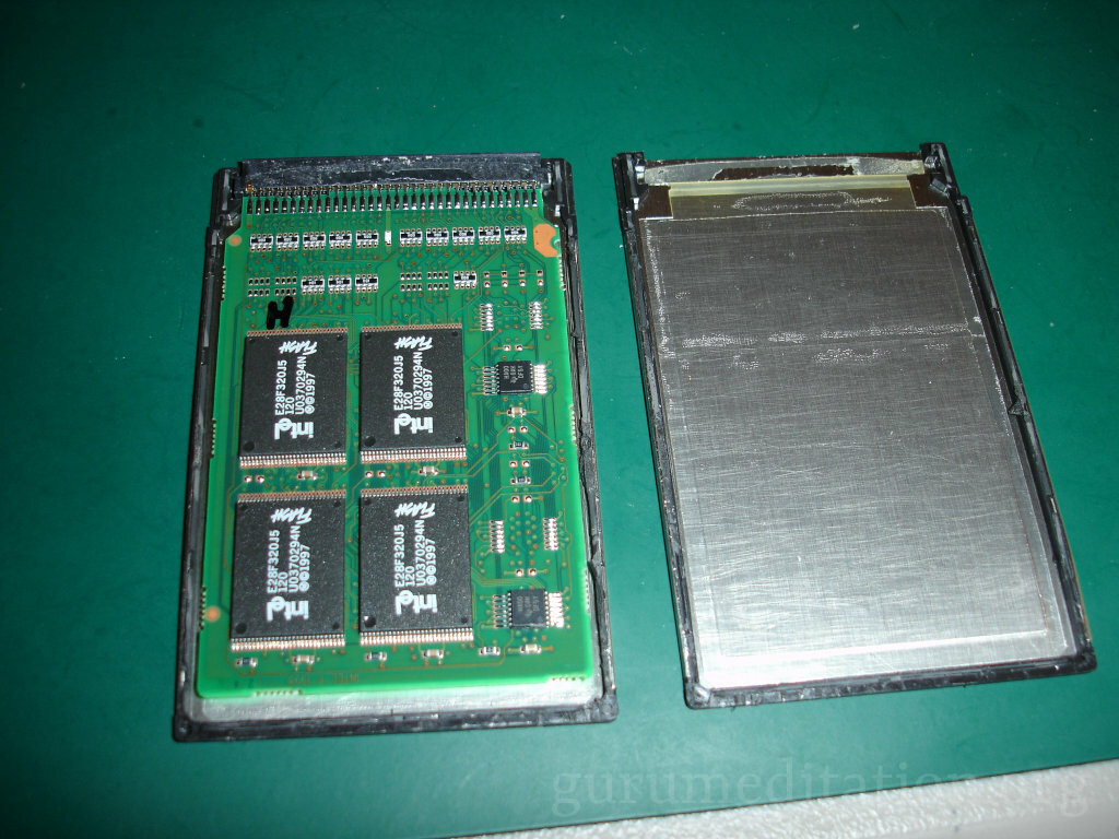
Now on to the meat of my project. I wanted to use a much cheaper and readily available PCMCIA linear flash card. 24MB $19 off eBay. Anything 2MB or larger will work. The 2MB requirement is because of the size of the firmware image if you want to boot the scope off the memory card. Older scopes may be able to use smaller cards if they have smaller firmware images.
The problem with most linear flash cards is that they are 16-bit only and need to be modified. On these cards the A0 line is not used except for the CFI. This can be solved many ways. First I’ll describe possible techniques that I didn’t use.
One way would be to disconnect a higher address pin on the card and connect it to A0. This way when the 8-bit A0 line is toggled it will select either “low memory” or “high memory”, simulating 8-bit access. This will reduce the capacity of the memory to half of its original size (or less) because the data on the card will need to be padded, only even addresses will be used. You will also need a switch of some sort so the card can be put back in to 16-bit mode for writing (padded) data to it. This should work on pretty much any memory card because you’re simply modifying the addressing scheme.
Many flash memory chips support both 8-bit and 16-bit access by use of a “BYTE#” pin on the chip. If this pin is disconnected from whatever hardware controls it on the card then it can be accessed.
It should be possible to connect and invert the CE2# line on the card to the BYTE# line(s) on the flash memory chips to have it automatically switch between 8-bit and 16-bit mode. I’m not sure why linear flash cards are not built with this capability in the first place since it’s not complex but I guess the cost of extra routing and such is not worth it. Maybe there are other issues I don’t understand.
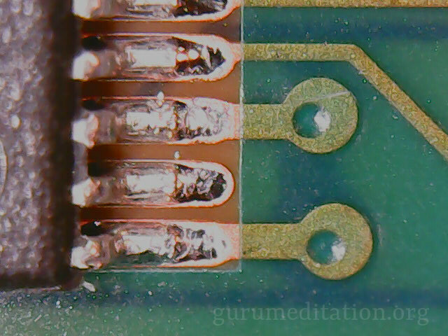
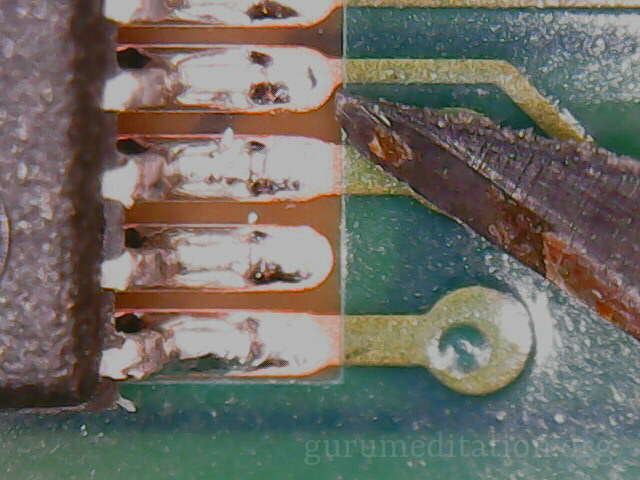
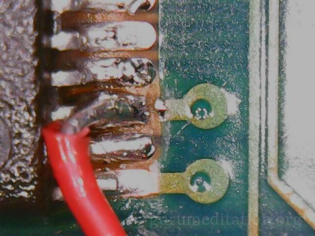
The approach I did take was the easy solution and that is to simply connect the BYTE# pin(s) to ground, converting the card to 8-bit only mode. To connect it to ground I first had to disconnect it from the power plane (see below).
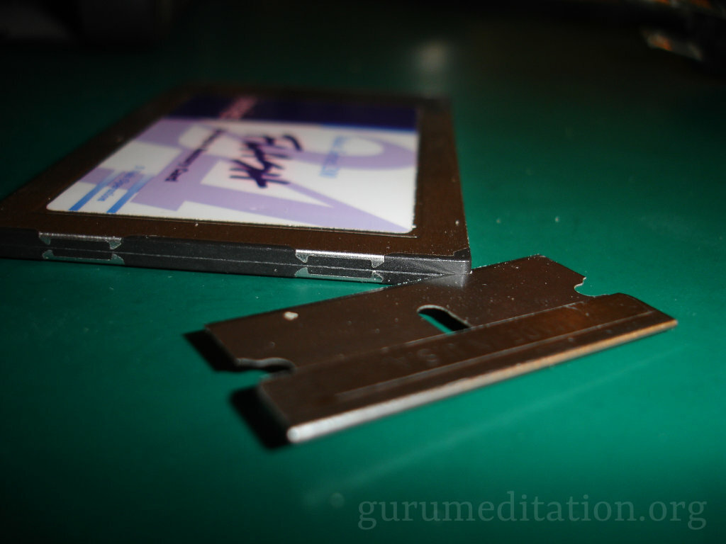
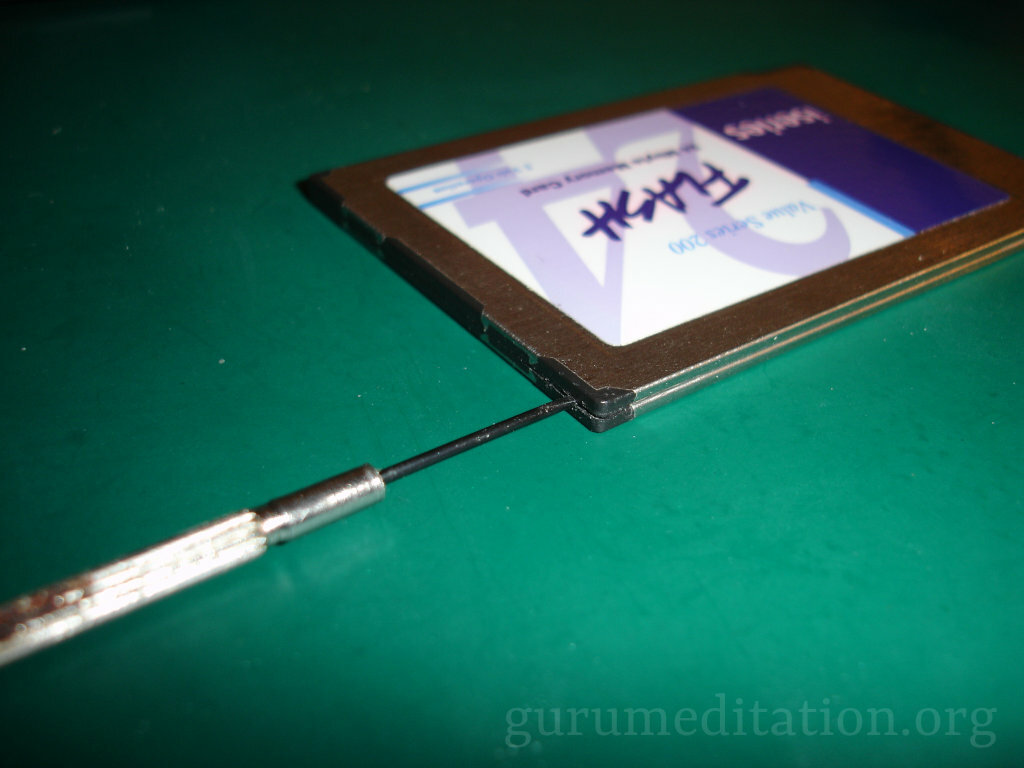
Opening most PCMCIA cards is not too difficult but you need to be careful. Bending the metal case in any way can be really hard to correct, preventing the card from being inserted in to tight sockets. Both the PCMCIA card I gutted and my linear flash card use a “split case” design where the metal can stay in place and the two plastic halves can be separated. Be careful when separating the plastic because there are usually plastic pins and/or grooves that anchor the two plastic halves:
This would be difficult without a microscope. Here is a picture of the modifications:
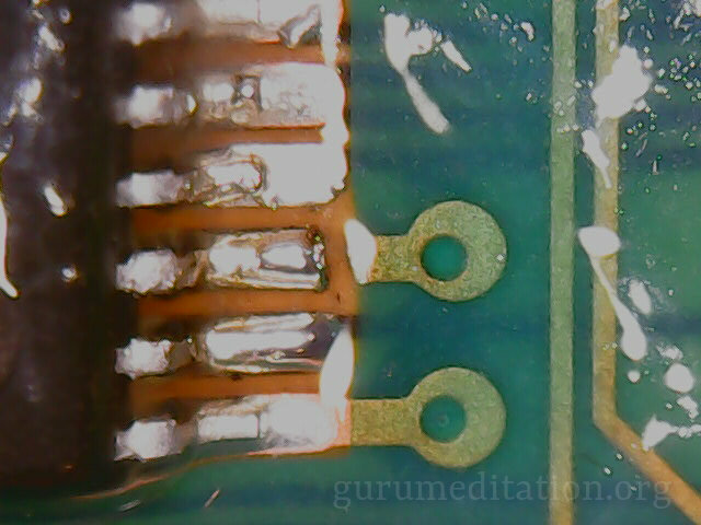
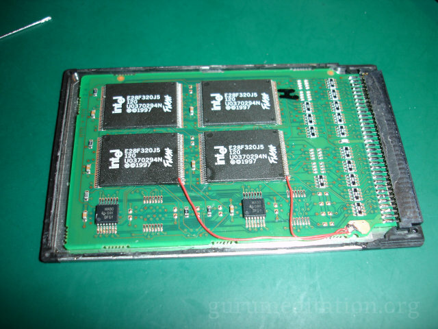
I only modified the first two 4MB chips, effectively making my card an 8MB card but since I only need 2MB even one chip is more than enough.
To put the card case back together I just used hot-glue. The original adhesive was really nice stuff. It’s thin and very strong while still being removable. I wish I knew where to get some of that stuff. Anyway, for the hot-glue I cut a thin sliver of glue and placed it between the two halves of plastic. I then heated the area with hot air until the glue melted then quickly clamped the two halves together until the glue set. I did this on all 4 corners. The glue is soft enough to remove if you need to get back in to the card plus you can just reheat it and clamp again to stick it back together.
If your card does not have attributes you may have problems accessing it in some operating systems. Special drivers may be required. On Linux however it’s not too difficult. First you need to enable anonymous memory devices in the kernel (this may require compiling a custom kernel). This is done with the CONFIG_MTD_PCMCIA_ANONYMOUS switch. Then the options of the pcmciamtd kernel module need to be controlled when it is loaded to force 8-bit mode. This is done with the “bankwidth=1” module option. You can also use the “mem_type=1” and “force_size=64” options to force the card to be detected as SRAM and its size. Writing to flash won’t work in SRAM mode but this is useful for testing to make sure your card it going to show up properly on the scope.
Usually right after I boot my Linux system I remove the pcmciamtd kernel and reload it with the option I want before I insert the card:
modprobe -r pcmciamtd
modprobe pcmciamtd bankwidth=1
# << insert flash card >>

# Or
modprobe -r pcmciamtd
modprobe pcmciamtd bankwidth=1 mem_type=1 mem_size=24
# << insert SRAM card>>
The kernel will probe probe for CFI/JEDEC information on flash memory devices so should be able to determine the write interface without any attributes present. Beware if you’re using an actual SRAM card because the kernel flash device probing will corrupt data on your card.
A note about flash memory. Flash memory can be written to at any time the blocks are unlocked. Unlocking is handled automatically by the kernel when writing. However, bits can only be changed from one (1) to zero (0). The only way to change a bit from zero to one is to erase the whole memory block (minimum size determined by the flash chip). So it’s possible to write zero bits to flash memory without doing anything special, you don’t necessarily need to erase. If you do need to erase a block then you will need to do it manually by using a utility such as flash_erase or mtd_debug. Flash memory has a limited number of erase cycles before it will fail. Especially these old linear flash devices may only last 10000 cycles or less so watch what you’re doing. If, like me, you only need 2MB of memory then that is the only part that will need to be erased. If that part wears out then I can simply change the address lines to use the second half of the 4MB chip. If that whole chip wears out then I can change the address lines on the 3-to-8 decoder on the flash card to use the next memory chip. In my case this gives me twelve 2MB areas for the life of this card. I doubt I will wear out one. If you have a flash card with bad memory areas these techniques can be used to bypass them.
Of course it’s possible to build your own SRAM or flash memory card but it hardly seems worth it when linear flash cards are easily available. However, many old scrapped devices like cable modems, routers, access points, etc have lots of flash memory in them so it should be possible to salvage them in to your own card. Might require some Linux hacking depending on the type of flash chip in order to write to it.
73
One response to “LeCroy Oscilloscope Memory Cards”
Any updates to your LeCroy O’Scope memory card article? I just got an LC574AL and Would like to try a memory card. I don’t mind doing some soldering. Thanks! Will in Grand Junction CO